beautypg.com
Manuals
Brands
Advantech Manuals
PCI Card
PCI-1718HGU
Advantech PCI-1718HGU Manuals
Manuals and User Guides for Advantech PCI-1718HGU. We have
1
Advantech PCI-1718HGU manual available for free PDF download: User Manual
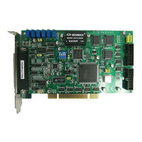
Advantech PCI-1718HGU User Manual (94 pages)
PCI-1718 Series 12-bit Multifunction Cards with Universal PCI Bus
Brand:
Advantech
| Category:
PCI Card
| Size: 1.62 MB
Table of Contents
Table of Contents
5
Chapter 1 Introduction
10
Features
11
Applications
12
Installation Guide
13
Figure 1.1:Installation Flow Chart
14
Software Overview
15
Device Driver Programming Roadmap
16
Accessories
18
Chapter 2 Installation
20
Unpacking
20
Driver Installation
21
Ware
21
Figure 2.1:Setup Screen of Advantech Automation Soft Ware
22
Figure 2.2:Different Options for Driver Setup
22
Hardware Installation
23
Device Setup & Configuration
24
Figure 2.3:The Device Manager Dialog Box
24
Figure 2.4:The Device Setting Dialog Box
25
Figure 2.5:Device Name Appearing on the List of Devic es Box
25
Figure 2.6:The Test Utility Dialog Box
26
Signal Connections
27
Chapter 3 Signal Connections
28
Overview
28
Switch and Jumper Settings
28
Setting the Boardid Switch (SW1)
29
Table 3.1:Board ID Setting (SW1)
29
Channel Configuration, S/E or DIFF (SW2)
30
Table 3.2:Summary of Switch SW2 Settings
30
D/A Reference Voltage, Int./Ext. (JP11)
30
Table 3.3:Summary of Jumper JP11 Settings
30
Internal Voltage Reference, -10 V or -5 V (JP10)
31
Table 3.4:Summary of Jumper JP10 Settings
31
Timer Clock Selection (JP8)
32
Table 3.5:Summary of Jumper JP8 Settings
32
Ext. Trigger and Counter Gate 0 Control (JP5)
33
Table 3.6:Summary of Jumper Settings
33
Digital Output, 20-Pin or 37-Pin Connector (JP1)
33
Table 3.7:Summary of Jumper Settings
34
Setting the Time to Reset Digital Outputs
35
Table 3.8:JP21 Jumper Settings
35
Signal Connections
36
1718 Series
36
I/O Connector Signal Description
37
Table 3.9:I/O Connector Signal Descriptions
37
Analog Input Connections
38
Figure 3.3:Analog Output Connections
41
Digital Signal Connections
42
Field Wiring Considerations
43
Chapter 4 Programming Guide
46
Overview
46
Programming with the Driver
46
Register Programming
46
Software Trigger and Polling
47
Pacer Trigger Mode with Interrupt
49
Pacer Trigger Mode with Interrupt and FIFO
53
Programming with Labview and Activedaq
57
Appendix A Specifications
60
Analog Input
60
A.1 Analog Input
60
Analog Output
61
A.2 Analog Output
61
Digital Input
62
Digital Output
62
A.3 Digital Input
62
A.4 Digital Output
62
Counter/Timer
63
A.5 Counter/Timer
63
General
64
A.6 General
64
Appendix B Block Diagrams
66
Appendix C Register Structure & Format
68
Overview
68
I/O Port Address Map
68
C.1 Overview
68
C.2 I/O Port Address Map
68
A/D Data and Channels - BASE+00H~01H
72
Software A/D Trigger - BASE+00H
72
C.3 A/D Data and Channels — BASE+00H~01H
72
C.4 Software A/D Trigger — BASE+00H
72
Table C.4:Register for A/D Data and Channels
72
Table C.5:Register for Software A/D Trigger
72
A/D Range Control - BASE+01H
73
C.5 A/D Range Control — BASE+01H
73
Table C.6:Register for A/D Range Control
73
MUX Scan Channel Control - BASE+02H
75
Table C.7:Register for MUX Scan Channel Control
75
MUX Scan Channel Status - BASE+02H
76
Table C.8:Register for MUX Scan Channel Status
76
Digital I/O Registers - BASE + 03/0BH
76
Table C.9:Register for Digital Output
76
D/A Output - BASE+04/05H
77
Table C.10:Register for Digital Output
77
C.9 D/A Output — BASE+04/05H
77
Table C.11:Register for D/A Output
77
FIFO Interrupt Control - BASE+06H
78
PCI-1718 Series User Manual
78
C.10 FIFO Interrupt Control — BASE+06H
78
Table C.12:Register for FIFO Interrupt Control
78
Clear Interrupt Request - BASE+08H
79
A/D Status - BASE+08H
79
C.11 Clear Interrupt Request — BASE+08H
79
C.12 A/D Status — BASE+08H
79
Table C.13:Register for Clear Interrupt Request
79
Table C.14:Register for A/D Status
79
A/D Control - BASE+09H
81
C.13 A/D Control — BASE+09H
81
Table C.15:Register for A/D Control
81
Timer/Counter Enable - BASE+0AH
82
Programmable Timer/Counter - BASE+0C~0FH
82
C.14 Timer/Counter Enable — BASE+0AH
82
C.15 Programmable Timer/Counter — BASE+0C~0FH
82
Table C.16:Register for Timer/Counter Enable
82
Clear FIFO Interrupt Request - BASE+14H
83
Table C.17:Register for Clear FIFO Interrupt Request
83
A/D Data and Channel from FIFO - BASE + 17/18H
83
Table C.18:Register for A/D Data and Channel from FIFO
83
Fifo
84
FIFO Status - BASE+19H
84
FIFO Clear - BASE+19H
84
C.18 FIFO Status — BASE+19H
84
C.19 FIFO Clear — BASE+19H
84
Table C.19:Register for FIFO Status
84
Table C.20:Register for FIFO Clear
84
Register Programming Flow Chart
85
Software Trigger Mode with Polling
85
Pacer Trigger Mode with Interrupt
86
Pacer Trigger Mode with Interrupt [FIFO Used]
87
Appendix D Calibration
90
VR Assignment
91
D.1 VR Assignment
91
Figure D.1:PCI-1718 VR Assignment
91
A/D Calibration
92
D.2 A/D Calibration
92
D/A Calibration
93
D.3 D/A Calibration
93
Related Products
Advantech PCI-1718 Series
Advantech PCI-1718HDU
Advantech PCI-1711U Series
Advantech PCI-1710HGL
Advantech PCI-1711L
Advantech PCI-1716
Advantech PCI-1714
Advantech PCI-1710U-DE
Advantech PCI-1713U
Advantech PCI-1714UL
Advantech Categories
Motherboard
Computer Hardware
Desktop
Touch Panel
PCI Card
More Advantech Manuals