beautypg.com
Manuals
Brands
Fujitsu Manuals
Microcontrollers
MB90460 Series
Fujitsu MB90460 Series Manuals
Manuals and User Guides for Fujitsu MB90460 Series. We have
1
Fujitsu MB90460 Series manual available for free PDF download: Hardware Manual
Fujitsu MB90460 Series Hardware Manual (739 pages)
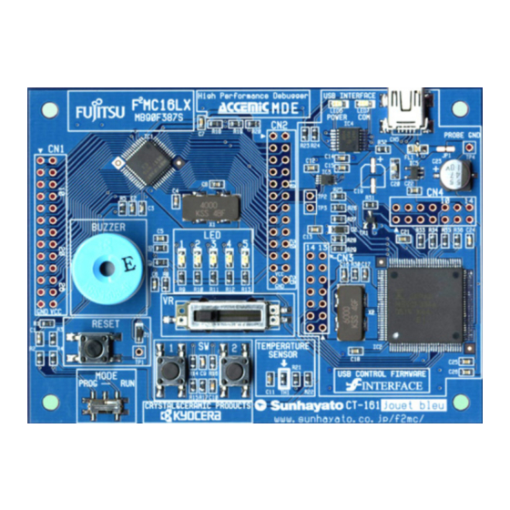
F2MC-16LX 16-BIT MICROCONTROLLER
Brand:
Fujitsu
| Category:
Microcontrollers
| Size: 6.21 MB
Table of Contents
Table of Contents
10
Chapter 1 Overview
20
MB90460/465 Series Features
21
MB90460/465 Series Product Line-Up
24
Block Diagram of MB90460/465 Series
26
Pin Assignment
27
Package Dimensions
30
I/O Pins and Pin Functions
33
I/O Circuit Types
38
Chapter 2 Notes on Handling Devices
42
Notes on Handling Devices
43
Chapter 3 Cpu
46
Cpu
47
Memory Space
48
Memory Maps
50
Addressing
52
Address Specification by Linear Addressing
53
Address Specification by Bank Addressing
54
Memory Location of Multi-Byte Data
56
Registers
58
Dedicated Registers
59
Accumulator (A)
61
Stack Pointers (USP, SSP)
64
Processor Status (PS)
66
Condition Code Register (PS: CCR)
67
Register Bank Pointer (PS: RP)
69
Interrupt Level Mask Register (PS: ILM)
70
Program Counter (PC)
71
Direct Page Register (DPR)
72
Bank Registers (PCB, DTB, USB, SSB, ADB)
73
General-Purpose Registers
74
Prefix Codes
76
Bank Select Prefix (PCB, DTB, ADB, SPB)
77
Common Register Bank Prefix (CMR)
79
Flag Change Suppression Prefix (NCC)
80
Restrictions on Prefix Codes
81
Chapter 4 Reset
84
Reset
85
Reset Causes and Oscillation Stabilization Wait Intervals
87
External Reset Pin
88
Reset Operation
90
Reset Cause Bits
92
Status of Pins in a Reset
94
Chapter 5 Clock
96
Clock
97
Block Diagram of the Clock Generation Block
99
Clock Selection Register (CKSCR)
101
Clock Mode
103
Oscillation Stabilization Wait Interval
105
Connection of an Oscillator or an External Clock to the Microcontroller
106
Chapter 6 Low Power Consumption Mode
108
Low Power Consumption Mode
109
Block Diagram of the Low Power Consumption Control Circuit
111
Low Power Consumption Mode Control Register (LPMCR)
113
CPU Intermittent Operation Mode
116
Standby Mode
117
Sleep Mode
118
Time-Base Timer Mode
121
Stop Mode
123
State Change Diagram
125
State of Pins in Standby Mode and During Reset
128
Usage Notes on Low Power Consumption Mode
129
Chapter 7 Interrupt
132
Interrupt
133
Interrupt Causes and Interrupt Vectors
135
Interrupt Control Registers and Peripheral Functions
138
Interrupt Control Registers (ICR00 to ICR15)
140
Interrupt Control Register Functions
142
Hardware Interrupt
145
Operation of Hardware Interrupt
148
Processing for Interrupt Operation
150
Procedure for Using Hardware Interrupt
151
Multiple Interrupts
152
Hardware Interrupt Processing Time
154
Software Interrupt
156
Interrupt of Extended Intelligent I/O Service (EI 2 OS)
158
Extended Intelligent I/O Service (EI 2 OS) Descriptor (ISD)
160
Registers of EI 2 os Descriptor (ISD)
161
Operation of the Extended Intelligent I/O Service (EI 2 OS)
164
Procedure for Using the Extended Intelligent I/O Service (EI 2 OS)
165
Processing Time of the Extended Intelligent I/O Service (EI 2 OS)
166
Exception Processing Interrupt
168
Stack Operations for Interrupt Processing
169
Sample Programs for Interrupt Processing
171
Chapter 8 Mode Setting
176
Mode Setting
177
Mode Pins (MD2 to MD0)
178
Mode Data
179
Chapter 9 I/O Port
182
Overview of I/O Port
183
Registers of I/O Port
185
Port 0
186
Port 0 Registers (PDR0, DDR0 and RDR0)
188
Operation of Port 0
190
Port 1
192
Port 1 Registers (PDR1, DDR1 and RDR1)
194
Operation of Port 1
195
Port 2
197
Port 2 Registers (PDR2 and DDR2)
199
Operation of Port 2
200
Port 3
202
Port 3 Registers (PDR3 and DDR3)
204
Operation of Port 3
205
Port 4
207
Port 4 Registers (PDR4 and DDR4)
209
Operation of Port 4
210
Port 5
212
Port 5 Registers (PDR5, DDR5 and ADER)
214
Operation of Port 5
215
Port 6
217
Port 6 Registers (PDR6 and DDR6)
219
Operation of Port 6
220
Sample I/O Port Program
222
Chapter 10 Time-Base Timer
224
Overview of the Time-Base Timer
225
Configuration of the Time-Base Timer
227
Time-Base Timer Control Register (TBTC)
228
Time-Base Timer Interrupts
230
Operation of the Time-Base Timer
231
Usage Notes on the Time-Base Timer
233
Sample Program for the Time-Base Timer Program
235
Chapter 11 Watchdog Timer
238
Overview of the Watchdog Timer
239
Configuration of the Watchdog Timer
240
Watchdog Timer Control Register (WDTC)
241
Operation of the Watchdog Timer
243
Usage Notes on the Watchdog Timer
245
Sample Program for the Watchdog Timer
246
Chapter 12 16-Bit Reload Timer
248
Overview of the 16-Bit Reload Timer
249
Block Diagram of the 16-Bit Reload Timer
252
16-Bit Reload Timer Pins
254
16-Bit Reload Timer Registers
255
Timer Control Status Register, Upper Byte (TMCSRH0/TMCSRH1)
256
Timer Control Status Register, Lower Byte (TMCSRL0/TMCSRL1)
258
16-Bit Timer Register (TMR0/TMR1)
260
16-Bit Reload Register (TMRD0/TMRD1)
261
16-Bit Reload Timer Interrupts
262
Operation of the 16-Bit Reload Timer
263
Internal Clock Mode (Reload Mode)
265
Internal Clock Mode (Single-Shot Mode)
267
Event Count Mode
269
Usage Notes on the 16-Bit Reload Timer
271
Sample Programs for the 16-Bit Reload Timer
272
Chapter 13 16-Bit Ppg Timer
276
Overview of 16-Bit PPG Timer
277
Block Diagram of 16-Bit PPG Timer
278
16-Bit PPG Timer Pins
279
16-Bit PPG Timer Registers
281
PPG down Counter Register (PDCR0 to PDCR2)
283
PPG Period Setting Buffer Register (PCSR0 to PCSR2)
284
PPG Duty Setting Buffer Register (PDUT0 to PDUT2)
285
PPG Control Status Register (PCNTL0 to PCNTL2, PCNTH0 to PCNTH2)
286
16-Bit PPG Timer Interrupts
290
Operation of 16-Bit PPG Timer
292
Usage Notes on the 16-Bit PPG Timer
295
Sample Programs for the 16-Bit PPG Timer
296
Chapter 14 Multi-Functional Timer
298
Overview of Multi-Functional Timer
299
Block Diagram of Multi-Functional Timer
301
Multi-Functional Timer Pins
305
Registers of Multi-Functional Timer
308
Compare Clear Buffer Register (CPCLRB) and Compare Clear Register (CPCLR)
312
Timer Data Register (TCDT)
313
Timer Control Status Register (TCCSH, TCCSL)
314
Output Compare Buffer Registers (OCCPB0 to OCCPB5) / Output Compare Registers (OCCP0 to OCCP5)
318
Compare Control Registers (OCS0 to OCS5)
320
Input Capture Register (IPCP0 to IPCP3)
324
Input Capture Control Status Registers (ICS23, PICS01)
325
16-Bit Timer Register (TMRR0/TMRR1/TMRR2)
332
16-Bit Timer Control Register (DTCR0/DTCR1/DTCR2)
333
Waveform Control Register (SIGCR)
337
Multi-Functional Timer Interrupts
339
Operation of Multi-Functional Timer
343
Operation of 16-Bit Free-Run Timer
344
Operation of 16-Bit Output Compare
351
Operation of 16-Bit Input Capture
356
Operation of Waveform Generator
358
Usage Notes on the Multi-Functional Timer
368
Sample Programs for the Multi-Functional Timer
370
Chapter 15 Multi-Pulse Generator
374
Overview of Multi-Pulse Generator
375
Block Diagram of Multi-Pulse Generator
378
Multi-Pulse Generator Pins
386
Registers of Multi-Pulse Generator
388
Output Control Register (OPCR)
391
Output Data Register (OPDR)
395
Output Data Buffer Register (OPDBR)
399
Input Control Register (IPCR)
403
Compare Clear Register (CPCR)
407
Timer Buffer Register (TMBR)
408
Timer Control Status Register (TCSR)
409
Noise Cancellation Control Register (NCCR)
411
Multi-Pulse Generator Interrupts
413
Operation of Multi-Pulse Generator
416
Operation of Position Detection
418
Operation of Data Write Control Unit
420
Operation of Output Data Buffer Register
424
Operation of Data Transfer of Output Data Register
426
Operation of DTTI1 Input Control
440
Operation of Noise Cancellation Function
443
Operation of 16-Bit Timer
444
Usage Notes on the Multi-Pulse Generator
448
Sample Programs for the Multi-Pulse Generator
450
CHAPTER 16 PWC Timer
452
Overview of the PWC Timer
453
Block Diagram of the PWC Timer
454
PWC Timer Pins
455
PWC Timer Registers
457
PWC Control Status Register (PWCSH0/PWCSH1, PWCSL0/PWCSL1)
458
PWC Data Buffer Register (PWC0/PWC1)
462
Division Rate Control Register (DIV0/DIV1)
463
PWC Timer Interrupts
464
Operation of the PWC Timer
466
Operation Mode Selection
469
Starting and Stopping the Timer and Pulse-Width Measurement and Clearing the Timer
470
Timer Mode Operation
472
Pulse Width Measurement Mode Operation
475
Usage Notes on the PWC Timer
480
Sample Programs for the PWC Timer
483
Chapter 17 Uart
486
Overview of UART
487
Block Diagram of UART
489
UART Pins
492
UART Registers
494
Serial Control Register (SCR0/SCR1)
495
Serial Mode Register (SMR0/SMR1)
497
Serial Status Register (SSR0/SSR1)
499
Input Data Register (SIDR0/SIDR1) and Output Data Register (SOR0/SOR1)
501
Communication Prescaler Control Register (CDCR)
503
UART Interrupts
505
Reception Interrupt Generation and Flag Set Timing
507
Transmission Interrupt Generation and Flag Set Timing
508
UART Baud Rates
509
Baud Rates Determined Using the Dedicated Baud Rate Generator
511
Baud Rates Determined Using the Internal Timer (16-Bit Reload Timer 0)
514
Baud Rates Determined Using the External Clock
516
Operation of UART
517
Operation in Asynchronous Mode (Operation Modes 0 and 1)
519
Operation in Synchronous Mode (Operation Mode 2)
521
Bidirectional Communication Function (Normal Mode)
523
Master-Slave Communication Function (Multiprocessor Mode)
525
Usage Notes on UART
528
Sample Program for UART
529
Chapter 18 Dtp/External Interrupt Circuit
532
Overview of the Dtp/External Interrupt Circuit
533
Block Diagram of the Dtp/External Interrupt Circuit
535
Dtp/External Interrupt Circuit Pins
537
Dtp/External Interrupt Circuit Registers
539
Dtp/Interrupt Cause Register (EIRR)
540
Dtp/Interrupt Enable Register (ENIR)
541
Request Level Setting Register (ELVR)
543
Operation of the Dtp/External Interrupt Circuit
544
External Interrupt Function
547
DTP Function
548
Usage Notes on the Dtp/External Interrupt Circuit
549
Sample Programs for the Dtp/External Interrupt Circuit
551
Chapter 19 Delayed Interrupt Generator Module
554
Overview of the Delayed Interrupt Generator Module
555
Delayed Interrupt Generator Module Register
556
Operation of the Delayed Interrupt Generator Module
557
Usage Notes on the Delayed Interrupt Generator Module
558
Chapter 20 8/10-Bit A/D Converter
561
Overview of the 8/10-Bit A/D Converter
561
Block Diagram of the 8/10-Bit A/D Converter
563
8/10-Bit A/D Converter Pins
565
8/10-Bit A/D Converter Registers
567
A/D Control Status Register 1 (ADCS1)
568
A/D Control Status Register 0 (ADCS0)
570
A/D Data Register (ADCR0/ADCR1)
573
8/10-Bit A/D Converter Interrupts
575
Operation of the 8/10-Bit A/D Converter
576
Conversion Using EI 2 os
579
A/D Conversion Data Protection Function
580
Usage Notes on the 8/10-Bit A/D Converter
582
Sample Program 1 for the 8/10-Bit A/D Converter (Single Conversion Mode Using EI 2 OS)
583
Sample Program 2 for the 8/10-Bit A/D Converter (Continuous Conversion Mode Using EI 2 OS)
585
Sample Program 3 for the 8/10-Bit A/D Converter (Stop Conversion Mode Using EI OS)
587
Chapter 21 Rom Correction Function
590
Overview of the ROM Correction Function
591
Block Diagram of ROM Correction Function
592
ROM Correction Function Registers
593
Program Aaddress Detection Register (PADR0/PADR1)
594
Program Address Detection Control Status Register (PACSR)
595
Operation of the ROM Correction Function
597
Example of Using ROM Correction Function
598
Chapter 22 Rom Mirroring Function Selection Module
602
Overview of the ROM Mirroring Function Selection Module
603
ROM Mirroring Function Selection Register (ROMM)
604
Chapter 23 512K / 1024K Bit Flash Memory
606
Overview of the 512K / 1024K Bit Flash Memory
607
1024K Bit Flash Memory Sector Configuration
608
Flash Memory Control Status Register (FMCS)
609
Method of Starting the Automatic Algorithm in Flash Memory
611
Verifying Automatic Algorithm Execution Status
612
Data Polling Flag (DQ7)
614
Toggle Bit Flag (DQ6)
616
Time Limit Exceeded Flag (DQ5)
617
Sector Deletion Timer Flag (DQ3)
618
Detailed Explanation on the Flash Memory Write/Delete
619
Setting the Read/Reset Status
620
Writing the Data
621
Deleting the Data (Chip Deletion)
623
Deleting the Data (Sector Deletion)
624
Temporarily Stopping the Sector Deletion
626
Restarting the Sector Deletion
627
Flash Security Feature
628
Programming Example of 512K Bit Flash Memory
629
Chapter 24 Example of F
634
MC-16Lx Mb90F462/F462A/F463A Connection for Serial Writing
634
Standard Configuration for Serial On-Board Writing (Fujitsu Standard)
635
Example of Connection for Serial Writing (When Power Supplied by User)
637
Example of Connection for Serial Writing (When Power Supplied from Writer)
639
Example of Minimum Connection with Flash Microcontroller Programmer (When Power Supplied by User)
641
Example of Minimum Connection with Flash Microcontroller Programmer (When Power Supplied from Writer)
643
Appendix
646
Appendix A I/O Map
647
APPENDIX B Instructions
654
Instruction Types
655
Addressing
656
Direct Addressing
658
Indirect Addressing
664
Execution Cycle Count
672
Effective Address Field
675
How to Read the Instruction List
676
F 2 MC-16LX Instruction List
679
Instruction Map
693
Index
716
Related Products
Fujitsu MB90465 Series
Fujitsu MB90480 Series
Fujitsu MB90487B
Fujitsu MB90488B
Fujitsu MB90483B
Fujitsu MB904 Series
Fujitsu MB90420/5 (A) Series
Fujitsu MB90427A
Fujitsu MB90428
Fujitsu MB90428A
Fujitsu Categories
Air Conditioner
Laptop
Server
Scanner
Storage
More Fujitsu Manuals