beautypg.com
Manuals
Brands
Fujitsu Manuals
Storage
MHV2080BH
Fujitsu MHV2080BH Manuals
Manuals and User Guides for Fujitsu MHV2080BH. We have
4
Fujitsu MHV2080BH manuals available for free PDF download: Product Manual, Maintenance Manual, Brochure & Specs
Fujitsu MHV2080BH Product Manual (276 pages)
MHV Series, 2.5-inch hard disk drives
Brand:
Fujitsu
| Category:
Storage
| Size: 2.52 MB
Table of Contents
Revision History
3
Operating Environment
6
Important Alert Items
9
Manual Organization
11
Table of Contents
13
CHAPTER 1 Device Overview
23
Features
24
Functions and Performance
24
Adaptability
24
Interface
25
Device Specifications
26
Specifications Summary
26
Table 1.1 Specifications
26
Model and Product Number
27
Table 1.2 Examples of Model Names and Product Numbers
27
Power Requirements
28
Figure 1.1 Permissible Range of +5V Rise Slope
28
Figure 1.2 Negative Voltage at +5 V When Power Is Turned off
29
Table 1.3 Current and Power Dissipation
30
Environmental Specifications
31
Figure 1.3 Current Fluctuation (Typ.) at +5 V When Power Is Turned on
31
Table 1.4 Environmental Specifications
31
Acoustic Noise
32
Shock and Vibration
32
Table 1.5 Acoustic Noise Specification
32
Table 1.6 Shock and Vibration Specification
32
Reliability
33
Error Rate
34
Media Defects
34
Load/Unload Function
34
Recommended Power-Off Sequence
35
Advanced Power Management (APM)
35
Table 1.7 Advanced Power Management
36
Interface Power Management (IPM)
37
Host-Initiated Interface Power Management (HIPM)
37
Device-Initiated Interface Power Management (DIPM)
37
Restriction of Use of Hazardous Substances
38
Table 1.8 Interface Power Management
38
CHAPTER 2 Device Configuration
39
Device Configuration
40
Figure 2.1 Disk Drive Outerview
40
System Configuration
41
SATA Interface
41
Drive Connection
41
Figure 2.2 Drive System Configuration
41
CHAPTER 3 Installation Conditions
43
Dimensions
44
Figure 3.1 Dimensions
44
Mounting
45
Figure 3.2 Orientation
45
Figure 3.3 Mounting Frame Structure
46
Figure 3.4 Location of Breather
47
Figure 3.5 Surface Cover Temperature Measurement Points
48
Table 3.1 Surface Temperature Measurement Points and Standard Values
48
Figure 3.6 Service Area
49
Figure 3.7 Handling Cautions
50
Connections with Host System
51
Device Connector
51
Figure 3.8 Connector Locations
51
Signal Segment and Power Supply Segment
52
Connector Specifications for Host System
52
Figure 3.9 Power Supply Pins (CN1)
52
Table 3.2 the Recommended Connector Specifications for the Host System
52
SATA Interface Cable Connection
53
Note about SATA Interface Cable Connection
53
CHAPTER 4 Theory of Device Operation
55
Outline
56
Subassemblies
56
Disk
56
Spindle
56
Actuator
56
Air Filter
57
Circuit Configuration
57
Figure 4.1 Power Supply Configuration
58
Figure 4.2 Circuit Configuration
59
Power-On Sequence
60
Figure 4.3 Power-On Operation Sequence
60
Self-Calibration
61
Self-Calibration Contents
61
Execution Timing of Self-Calibration
62
Command Processing During Self-Calibration
62
Read/Write Circuit
63
Read/Write Preamplifier (Preamp)
63
Write Circuit
63
Figure 4.4 Read/Write Circuit Block Diagram
63
Read Circuit
64
Figure 4.5 Frequency Characteristic of Programmable Filter
64
Digital PLL Circuit
65
Servo Control
66
Servo Control Circuit
66
Figure 4.6 Block Diagram of Servo Control Circuit
66
Data-Surface Servo Format
69
Figure 4.7 Physical Sector Servo Configuration on Disk Surface
70
Servo Frame Format
71
Figure 4.8 Servo Frame Format
71
Actuator Motor Control
72
Spindle Motor Control
73
CHAPTER 5 Interface
75
Physical Interface
76
Interface Signals
76
Figure 5.1 Interface Signals
76
Signal Interface Regulation
78
Out of Band Signaling
78
Primitives Descriptions
79
Electrical Specifications
81
Table 5.1 Physical Layer Electrical Requirements
81
Connector Pinouts
84
Table 5.2 Connector Pinouts
84
P11 Function
85
Staggered Spin-Up
85
Driving Ready LED
85
Table 5.3 Requirements for P11 as an Output Pin
85
Figure 5.2 Example of the Circuit for Driving Ready LED
86
Hot Plug
87
Logical Interface
88
Figure 5.3 Conceptual Diagram of Communication Layers
88
Communication Layers
89
Outline of the Shadow Block Register
90
Table 5.4 Shadow Block Register
90
Outline of the Frame Information Structure (FIS)
91
FIS Types
91
Register - Host to Device
91
Figure 5.4 Register - Host to Device FIS Layout
91
Register - Device to Host
92
DMA Active - Device to Host
92
Figure 5.5 Register - Device to Host FIS Layout
92
Figure 5.6 DMA Active - Device to Host FIS Layout
92
DMA Setup - Device to Host or Host to Device (Bidirectional)
93
Figure 5.7 DMA Setup - Device to Host or Host to Device FIS Layout
93
BIST Active - Bidirectional
94
Figure 5.8 bist Active - Bidirectional FIS Layout
94
Table 5.5 bist Combinations
94
Data - Host to Device or Device to Host (Bidirectional)
95
Figure 5.10 PIO Setup - Device to Host FIS Layout
95
Figure 5.9 Data FIS (Bidirectional) Layout
95
PIO Setup - Device to Host
95
Figure 5.11 Set Device Bits FIS
97
Set Device Bits - Device to Host
97
Shadow Block Registers
98
Host Commands
103
Command Code and Parameters
103
Table 5.6 Command Code and Parameters
103
Command Descriptions
106
RECALIBRATE (X'10' to X'1F')
107
READ SECTOR(S) (X'20' or X'21')
108
WRITE SECTOR(S) (X'30' or X'31')
110
Write Verify (X'3C')
112
READ VERIFY SECTOR(S) (X'40' or X'41')
114
SEEK (X'70' to X'7F')
116
Execute Device Diagnostic (X'90')
117
Table 5.7 Diagnostic Code
117
Initialize Device Parameters (X'91')
118
Download Microcode (X'92')
119
Table 5.8 Operation of DOWNLOAD MICROCODE
119
Table 5.9 Example of Rewriting Procedure of Data 512K Bytes (80000H Bytes) of Microcode
120
STANDBY IMMEDIATE (X'94' or X'E0')
121
IDLE IMMEDIATE (X'95' or X'E1') /UNLOAD IMMEDIATE (X'95' or X'E1')
122
STANDBY (X'96' or X'E2')
124
IDLE (X'97' or X'E3')
125
CHECK POWER MODE (X'98' or X'E5')
127
SLEEP (X'99' or X'E6')
128
Smart (X'b0')
129
Table 5.10 Features Field Values (Subcommands) and Functions (1/3
130
Table 5.11 Format of Device Attribute Value Data
134
Table 5.12 Format of Guarantee Failure Threshold Value Data
134
Table 5.13 Off-Line Data Collection Status
137
Table 5.14 Self-Test Execution Status
137
Table 5.15 Off-Line Data Collection Capability
138
Table 5.16 Failure Prediction Capability Flag
138
Table 5.17 Drive Error Logging Capability
138
Table 5.18 Log Directory Data Format
139
Table 5.19 Data Format of SMART Summary Error Log
140
Table 5.20 Data Format of SMART Comprehensive Error Log
142
Table 5.21 SMART Self-Test Log Data Format
143
Table 5.22 Selective Self-Test Log Data Structure
144
Table 5.23 Selective Self-Test Feature Flags
145
Device Configuration (X'b1')
146
Table 5.24 DEVICE CONFIGURATION IDENTIFY Data Structure
149
Read Multiple (X'c4')
151
Figure 5.12 Execution Example of READ MULTIPLE Command
152
Write Multiple (X'c5')
154
Set Multiple Mode (X'c6')
156
READ DMA (X'C8' or X'C9')
158
WRITE DMA (X'CA' or X'CB')
160
Read Buffer (X'e4')
162
Flush Cache (X'e7')
163
Write Buffer (X'e8')
164
Identify Device (X'ec')
165
Identify Device Dma (X'ee')
166
Table 5.25 Information to be Read by IDENTIFY DEVICE Command
167
Set Features (X'ef')
178
Table 5.26 Features Field Values and Settable Modes
178
Security Set Password (X'f1')
184
Table 5.27 Contents of SECURITY SET PASSWORD Data
184
Security Unlock(X'f2')
186
Security Erase Prepare (X'f3')
188
Security Erase Unit (X'f4')
189
Security Freeze Lock (X'f5')
190
Security Disable Password (X'f6')
192
Table 5.29 Contents of Security Password
192
Read Native Max Address (X'f8')
194
Set Max (X'f9')
195
Read Sector (S) Ext (X'24')
201
Read Dma Ext (X'25')
202
Read Native Max Address Ext (X'27')
203
Read Multiple Ext (X'29')
204
Read Log Ext (X'2F')
205
Table 5.30 Data Format of Read Log Ext Log Page 10H
207
Table 5.31 Tag Field Information
207
Table 5.32 Data Format of Read Log Ext Log Page 11H
208
Table 5.33 Counter Identifier Information
208
Write Sector (S) Ext (X'34')
209
Write Dma Ext (X'35')
210
Set Max Address Ext (X'37')
211
Write Multiple Ext (X'39')
213
Write Log Ext (X'3F')
214
Read Verify Sector (S) Ext (X'42')
216
Flush Cache Ext (X'ea')
217
Write Multiple Fua Ext (X'ce')
218
Write Dma Fua Ext (X'3D')
219
Read Fp Dma Queued (X'60')
220
Write Fp Dma Queued (X'61')
221
Error Posting
222
Table 5.34 Command Code and Parameters
222
Command Protocol
224
Non-Data Command Protocol
224
Figure 5.13 Non-Data Command Protocol
225
PIO Data-In Command Protocol
226
PIO Data-Out Command Protocol
227
Figure 5.14 PIO Data-In Command Protocol
227
Figure 5.15 PIO Data-Out Command Protocol
228
DMA Data-In Command Protocol
229
Figure 5.16 DMA Data-In Command Protocol
229
DMA Data-Out Command Protocol
230
Figure 5.17 DMA Data-Out Command Protocol
230
Native Command Queuing Protocol
231
Figure 5.18 READ FP DMA QUEUED Command Protocol
232
Figure 5.19 WRITE FP DMA QUEUED Command Protocol
233
Power-On and COMRESET
234
Figure 5.20 Power-On Sequence
234
Figure 5.21 COMRESET Sequence
235
CHAPTER 6 Operations
237
Reset and Diagnosis
238
Response to Power-On
238
Response to COMRESET
240
Figure 6.3 Response to COMRESET
240
COMRESET Preservation Requirements
241
Software Settings Preservation
241
Response to a Software Reset
243
Figure 6.4 Response to a Software Reset
243
Power Save
244
Power Save Mode
244
Power Commands
246
Power Save Controlled by Interface Power Management (IPM)
247
Power Save Mode of the Interface
247
Read-Ahead Cache
249
Data Buffer Structure
249
Figure 6.5 Data Buffer Structure
249
Caching Operation
250
Using the Read Segment Buffer
252
Miss-Hit
252
Sequential Hit
253
Full Hit
253
Partial Hit
255
Write Cache
256
Cache Operation
256
Glossary
259
Acronyms and Abbreviations
263
Index
265
Fujitsu MHV2080BH Product Manual (274 pages)
MHV Series, 2.5-inch hard disk drives
Brand:
Fujitsu
| Category:
Storage
| Size: 2.69 MB
Table of Contents
For Safe Operation
2
Operating Environment
6
Table of Contents
13
CHAPTER 1 Device Overview
25
Features
26
Functions and Performance
26
Adaptability
26
Interface
27
Device Specifications
28
Specifications Summary
28
Table 1.1 Specifications
28
Model and Product Number
29
Table 1.2 Examples of Model Names and Product Numbers
29
Power Requirements
30
Figure 1.1 Negative Voltage at +5 V When Power Is Turned off
30
Table 1.3 Current and Power Dissipation
31
Environmental Specifications
32
Figure 1.2 Current Fluctuation (Typ.) at +5 V When Power Is Turned on
32
Table 1.4 Environmental Specifications
32
Acoustic Noise
33
Shock and Vibration
33
Table 1.5 Acoustic Noise Specification
33
Table 1.6 Shock and Vibration Specification
33
Reliability
34
Error Rate
35
Media Defects
35
Load/Unload Function
35
Recommended Power-Off Sequence
36
Advanced Power Management
36
Table 1.7 Advanced Power Management
37
Interface Power Management (IPM)
38
Host-Initiated Interface Power Management (HIPM)
38
Device-Initiated Interface Power Management (DIPM)
38
Elimination of Hazardous Substances
39
Table 1.8 Interface Power Management
39
CHAPTER 2 Device Configuration
41
Device Configuration
42
Figure 2.1 Disk Drive Outerview
42
System Configuration
43
SATA Interface
43
Drive Connection
43
Figure 2.2 Drive System Configuration
43
CHAPTER 3 Installation Conditions
45
Dimensions
46
Figure 3.1 Dimensions
46
Mounting
47
Figure 3.2 Orientation
47
Figure 3.3 Mounting Frame Structure
48
Figure 3.4 Location of Breather
49
Figure 3.5 Surface Cover Temperature Measurement Points
50
Table 3.1 Surface Temperature Measurement Points and Standard Values
50
Figure 3.6 Service Area
51
Figure 3.7 Handling Cautions
52
Connections with Host System
53
Device Connector
53
Figure 3.8 Connector Locations
53
Signal Segment and Power Supply Segment
54
Connector Specifications for Host System
54
Figure 3.9 Power Supply Pins (CN1)
54
Table 3.2 the Recommended Connector Specifications for the Host System
54
SATA Interface Cable Connection
55
Note about SATA Interface Cable Connection
55
CHAPTER 4 Theory of Device Operation
57
Outline
58
Subassemblies
58
Disk
58
Spindle
58
Actuator
58
Air Filter
59
Circuit Configuration
59
Figure 4.1 Power Supply Configuration
60
Figure 4.2 Circuit Configuration
61
Power-On Sequence
62
Figure 4.3 Power-On Operation Sequence
62
Self-Calibration
63
Self-Calibration Contents
63
Execution Timing of Self-Calibration
64
Command Processing During Self-Calibration
64
Read/Write Circuit
65
Read/Write Preamplifier (Preamp)
65
Write Circuit
65
Figure 4.4 Read/Write Circuit Block Diagram
65
Read Circuit
66
Figure 4.5 Frequency Characteristic of Programmable Filter
66
Digital PLL Circuit
67
Servo Control
68
Servo Control Circuit
68
Figure 4.6 Block Diagram of Servo Control Circuit
68
Index
69
Data-Surface Servo Format
71
Figure 4.7 Physical Sector Servo Configuration on Disk Surface
72
Servo Frame Format
73
Figure 4.8 Servo Frame Format
73
Actuator Motor Control
74
Spindle Motor Control
75
CHAPTER 5 Interface
77
Physical Interface
78
Interface Signals
78
Figure 5.1 Interface Signals
78
Signal Interface Regulation
80
Out of Band Signaling
80
Primitives Descriptions
81
Electrical Specifications
83
Table 5.1 Physical Layer Electrical Requirements
83
Connector Pinouts
86
Table 5.2 Connector Pinouts
86
P11 Function
87
Staggered Spin-Up
87
Driving Ready LED
87
Table 5.3 Requirements for P11 as an Output Pin
87
Figure 5.2 Example of the Circuit for Driving Ready LED
88
Hot Plug
89
Logical Interface
90
Figure 5.3 Conceptual Diagram of Communication Layers
90
Communication Layers
91
Outline of the Shadow Block Register
92
Table 5.4 Shadow Block Register
92
Figure 5.4 Register - Host to Device FIS Layout
93
FIS Types
93
Outline of the Frame Information Structure (FIS)
93
Register - Host to Device
93
DMA Active - Device to Host
94
Figure 5.5 Register - Device to Host FIS Layout
94
Figure 5.6 DMA Active - Device to Host FIS Layout
94
Register - Device to Host
94
DMA Setup - Device to Host or Host to Device (Bidirectional)
95
Figure 5.7 DMA Setup - Device to Host or Host to Device FIS Layout
95
BIST Active - Bidirectional
96
Figure 5.8 bist Active - Bidirectional FIS Layout
96
Table 5.5 bist Combinations
96
Data - Host to Device or Device to Host (Bidirectional)
97
Figure 5.9 Data FIS (Bidirectional) Layout
97
Shadow Block Registers
98
Host Commands
103
Command Code and Parameters
103
Table 5.6 Command Code and Parameters
103
Command Descriptions
106
RECALIBRATE (X'10' to X'1F')
107
READ SECTOR(S) (X'20' or X'21')
108
WRITE SECTOR(S) (X'30' or X'31')
110
Write Verify (X'3C')
112
READ VERIFY SECTOR(S) (X'40' or X'41')
114
SEEK (X'70' to X'7F')
116
Execute Device Diagnostic (X'90')
117
Table 5.7 Diagnostic Code
117
Initialize Device Parameters (X'91')
118
Download Microcode (X'92')
119
Table 5.8 Operation of DOWNLOAD MICROCODE
119
Table 5.9 Example of Rewriting Procedure of Data 512K Bytes (80000H Bytes) of Microcode
120
STANDBY IMMEDIATE (X'94' or X'E0')
121
IDLE IMMEDIATE (X'95' or X'E1')
122
STANDBY (X'96' or X'E2')
123
IDLE (X'97' or X'E3')
124
CHECK POWER MODE (X'98' or X'E5')
126
SLEEP (X'99' or X'E6')
127
Smart (X'b0')
128
Table 5.10 Features Field Values (Subcommands) and Functions (1/3
129
Table 5.11 Format of Device Attribute Value Data
133
Table 5.12 Format of Guarantee Failure Threshold Value Data
133
Table 5.13 Off-Line Data Collection Status
136
Table 5.14 Self-Test Execution Status
136
Table 5.15 Off-Line Data Collection Capability
137
Table 5.16 Failure Prediction Capability Flag
137
Table 5.17 Drive Error Logging Capability
137
Table 5.18 Log Directory Data Format
138
Table 5.19 Data Format of SMART Summary Error Log
139
Table 5.20 Data Format of SMART Comprehensive Error Log
141
Table 5.21 SMART Self-Test Log Data Format
142
Table 5.22 Selective Self-Test Log Data Structure
143
Table 5.23 Selective Self-Test Feature Flags
144
Device Configuration (X'b1')
145
Table 5.24 DEVICE CONFIGURATION IDENTIFY Data Structure
148
Read Multiple (X'c4')
150
Figure 5.10 Execution Example of READ MULTIPLE Command
151
Write Multiple (X'c5')
153
Set Multiple Mode (X'c6')
155
READ DMA (X'C8' or X'C9')
157
WRITE DMA (X'CA' or X'CB')
159
Read Buffer (X'e4')
161
Flush Cache (X'e7')
162
Write Buffer (X'e8')
163
Identify Device (X'ec')
164
Identify Device Dma (X'ee')
165
Table 5.25 Information to be Read by IDENTIFY DEVICE Command
166
Set Features (X'ef')
177
Table 5.26 Features Field Values and Settable Modes
177
Security Set Password (X'f1')
182
Table 5.27 Contents of SECURITY SET PASSWORD Data
182
Security Unlock(X'f2')
184
Security Erase Prepare (X'f3')
186
Security Erase Unit (X'f4')
187
Security Freeze Lock (X'f5')
188
Security Disable Password (X'f6')
190
Table 5.29 Contents of Security Password
190
Read Native Max Address (X'f8')
192
Set Max (X'f9')
193
Read Sector (S) Ext (X'24')
199
Read Dma Ext (X'25')
200
Read Native Max Address Ext (X'27')
201
Read Multiple Ext (X'29')
202
Read Log Ext (X'2F')
203
Table 5.30 Data Format of Read Log Ext Log Page 10H
205
Table 5.31 Tag Field Information
205
Table 5.32 Data Format of Read Log Ext Log Page 11H
206
Table 5.33 Counter Identifier Information
206
Write Sector (S) Ext (X'34')
207
Write Dma Ext (X'35')
208
Set Max Address Ext (X'37')
209
Write Multiple Ext (X'39')
211
Write Log Ext (X'3F')
212
Read Verify Sector (S) Ext (X'42')
214
Flush Cache Ext (X'ea')
215
Write Multiple Fua Ext (X'ce')
216
Write Dma Fua Ext (X'3D')
217
Read Fp Dma Queued (X'60')
218
Write Fp Dma Queued (X'61')
219
Error Posting
220
Table 5.34 Command Code and Parameters
220
Command Protocol
222
Non-Data Command Protocol
222
Figure 5.11 Non-Data Command Protocol
223
PIO Data-In Command Protocol
224
PIO Data-Out Command Protocol
225
Figure 5.12 PIO Data-In Command Protocol
225
Figure 5.13 PIO Data-Out Command Protocol
226
DMA Data-In Command Protocol
227
Figure 5.14 DMA Data-In Command Protocol
227
DMA Data-Out Command Protocol
228
Figure 5.15 DMA Data-Out Command Protocol
228
Native Command Queuing Protocol
229
Figure 5.16 READ FP DMA QUEUED Command Protocol
230
Figure 5.17 WRITE FP DMA QUEUED Command Protocol
231
Power-On and COMRESET
232
Figure 5.18 Power-On Sequence
232
Figure 5.19 COMRESET Sequence
233
CHAPTER 6 Operations
235
Reset and Diagnosis
236
Response to Power-On
236
Figure 6.2 Response to Power-On (When the Device Is Powered on Earlier than the Host)
237
Response to COMRESET
238
Figure 6.3 Response to COMRESET
238
COMRESET Preservation Requirements
239
Software Settings Preservation
239
Response to a Software Reset
241
Figure 6.4 Response to a Software Reset
241
Power Save
242
Power Save Mode
242
Power Commands
244
Power Save Controlled by Interface Power Management (IPM)
245
Power Save Mode of the Interface
245
Read-Ahead Cache
247
Data Buffer Structure
247
Figure 6.5 Data Buffer Structure
247
Caching Operation
248
Using the Read Segment Buffer
250
Miss-Hit
250
Sequential Hit
251
Full Hit
251
Partial Hit
253
Write Cache
254
Cache Operation
254
Glossary
257
Acronyms and Abbreviations
261
Fujitsu MHV2080BH Maintenance Manual (42 pages)
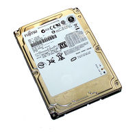
2.5-inch hard disk drives with a built-in controller
Brand:
Fujitsu
| Category:
Storage
| Size: 0.38 MB
Table of Contents
Revision History
3
Hot Plug
6
Operating Environment
6
Important Alert Items
9
Manual Organization
13
Table of Contents
15
CHAPTER 1 Maintenance and Diagnosis
17
Maintenance
18
Rules for Maintenance
18
Maintenance Requirements
19
Maintenance Levels
21
Disk Drive Revision Number
22
Figure 1.1 Disk Drive Revision Number Label
22
Figure 1.2 Display of Disk Drive Revision Number
23
Tools and Test Equipment
24
Self-Diagnostics
24
Test
24
Figure 1.3 Test Flowchart
25
Table 1.1 Status Field Contents
26
Table 1.2 Disposition for Error Field Contents
26
Operation Confirmation
27
Operation Test
27
Diagnostic Test
27
Troubleshooting Procedure
28
Troubleshooting Disk Drive Replaced in Field
28
Table 1.3 System Level and Field Troubleshooting
29
Troubleshooting at Factory
30
CHAPTER 2 Removal and Replacement Procedure
31
Spare Parts
32
Disk Drive Removal
32
Table 2.1 Model and Parts Numbers
32
Acronyms and Abbreviations
33
Fujitsu MHV2080BH Brochure & Specs (2 pages)
2.5-Inch, Serial ATA 5,400 RPM Mobile Hard Disk Drives
Brand:
Fujitsu
| Category:
Storage
| Size: 0.1 MB
Related Products
Fujitsu MHV2080AH - 80GB UDMA/100 5400RPM 8MB Notebook Hard Drive
Fujitsu MHV2080AT
Fujitsu MHV2080AS - Extended Duty Mobile 80 GB Hard Drive
Fujitsu MHV2080BS
Fujitsu MHV2080AH
Fujitsu MHV2040AT - Hard Drive - 40 GB
Fujitsu MHV2040AH - Mobile - Hard Drive
Fujitsu MHV2060AT
Fujitsu MHV2060BH
Fujitsu MHV2060AH
Fujitsu Categories
Air Conditioner
Laptop
Server
Scanner
Storage
More Fujitsu Manuals