beautypg.com
Manuals
Brands
SEMIKRON Manuals
Control Unit
20601238
SEMIKRON 20601238 Manuals
Manuals and User Guides for SEMIKRON 20601238. We have
1
SEMIKRON 20601238 manual available for free PDF download: Additional Explanation
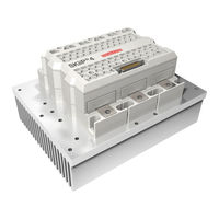
SEMIKRON 20601238 Additional Explanation (73 pages)
Brand:
SEMIKRON
| Category:
Control Unit
| Size: 8.53 MB
Table of Contents
Section 1
2
Table of Contents
2
1 Related Documents
4
2 Introduction
5
Figure 2.2: Half Bridge Definition
5
Heat Sink
6
Power Section
6
Figure 2.3: Half Bridge "Exploded Assembly View
6
Gate Drive Unit
7
Figure 2.4: Main Terminals Construction Principle
7
3 Topologies and Selection Guide
8
Type Designation Code
8
Overview of the Available Types and Current Ratings
9
Table 3-1: Skiip
9
4 Standards and Qualification Tests
10
Tests for Qualification and Re-Qualification
10
Electromagnetic Compatibility (EMC)
10
Table 4-1: Skiip
10
Table 4-2: Skiip
10
Isolation Coordination
11
Installation Altitude
11
Figure 4.1: Grounded Delta Grid
11
Figure 4.2: Star Grounded Circuit Network (690V-TN-Grid)
11
Table 4-3: Isolation Limits Skiip ® 4
11
Table 4-4: Altitude Correction Factors (IEC 60664-1)
12
Figure 4.3: Implementation of Additional Basic Isolation between Skiip
13
Figure 7.5: Skiip
14
Table 4-5: Installation Altitudes for Skiip
14
5 Gate Driver Board
15
Overview
15
Figure 5.1: Gate Driver Board Block Diagram
15
Gate Driver Interface "Skiface
16
Overview
16
Figure 5.2: Gate Driver Interface
16
Pin Description
17
Table 5-1: Pin Configuration Skiip ® 4
17
Figure 5.4: Overview Schematics Skiface Interface
19
External Power Supply
20
Table 5-2: Requirements to the Auxiliary Power Supply
20
Switching Signal Inputs
21
Figure 5.5: TOP/BOT PWM Signal Input
21
Figure 5.6: Threshold Level for HB_TOP and HB_BOT
21
Analogue Output Signals
22
Figure 5.7: Schematic View of the Analogue Output Signals
22
Figure 5.8: Application Example - Symmetric Wired Differential Amplifier. Terminal Description HB_I and
23
HALT Logic Signal
24
Figure 5.9: Application Example of the HALT Signal Processing for Separated Skiip
25
CMN_GPIO1 Signal
26
Figure 5.10: Application Example of the CMN_GPIO1 (Inverted HALT Signal) as Error Output Signal
26
Canbus Interface
27
Figure 5.11: CAN-Interface
27
Figure 5.12: CAN - Application Example for Several Skiip
27
Ground Connection
29
5.2.10 Shield and Protective Earth/Chassis Connection
29
Figure 5.13: Prevention of Ground Loops by Differential Amplifier Circuitry
29
Table 5-3: Ground Connections of Skiip ® 4
29
5.2.11 Reserved or Not Used Signals
30
Figure 5.14: Ground and Shield Connection. Principle Schematics for Ground and Shield Connection. Principle Equivalent Circuit of Switching Signal Inputs
30
Figure 5.15: Ground and Shield Connection. Principle Equivalent Circuit for Analogue Output Signals (Example: Temperature Output)
30
Gate Driver Board
31
Overview
31
Digital Signal Transmission
31
Power-On-Reset
31
Figure 5.16: Connection of Reserved and Not Used Signals at the User Controller Board
31
Interlock Dead Time Generation
32
Short Pulse Suppression
32
Figure 5.17: Power-On-Reset Timing Diagramm
32
Figure 5.18: Short Pulse Suppression
32
Intellioff
33
Figure 5.19 : Turn-Off Speed Scenarios
33
Table 5-4: Intellioff Functionality
34
Table 5-5: Power Loss Impact of Intellioff Operation
34
Error Management
35
Table 5-6: Error Delay Time
35
Table 5-7: Signal Characteristics of under Voltage Protection of the Primary Side
35
Figure 5.20: Switching Frequency Range
36
Figure 5.21: Timing Diagram for the TOP/BOT Overlapping Error Processing (T<3Μs)
36
Figure 5.22: Timing Diagram for the HB_TOP/HB_BOT Overlapping Error Processing (T>3Μs)
37
Analogue Signals / Sensor Functionality
38
Figure 5.23: no Short Circuit
38
Figure 5.24: Short Circuit During Operation
38
Figure 5.25: Short Circuit During Turn on
38
Table 5-8: Signal Characteristic of Current Measurement
38
Figure 5.29: Bode Diagram of the AC-Current Measurement at the Skiip4 Interface
41
Figure 5.30: Compensation Principle of Skiip
41
Figure 5.31: Characteristic between DCB-Sensor Temperature and the Voltage at CMN_TEMP
42
Table 5-9: Characteristics of the DCB-Temperature Sensor Circuit
42
Table 5-10
43
Figure 5.32: DC Link Voltage Sensor Output 1200V System
44
Figure 5.33: DC-Link Voltage Sensor Output 1700V System
44
Figure 5.34: Bode Diagram of the DC-Link Voltage Measurement at the Skiip4 Interface
45
6 Power Terminals
46
Electrical Limits
46
Mechanical Constraints
46
Torque at Terminal Connections
46
Table 6-1: Maximum Allowable Forces to Terminals
46
Figure 6.1: Maximum Forces at the Main Terminals
47
Figure 6.2: AC Connection
48
7 Application Hints
49
Verification of Design
49
Safe Operating Area for Skiip 4
49
Figure 7.1: Safe Operating Area for Standard Skiip ® 4
49
Maximum Blocking Voltage and Snubber Capacitors
50
Definition of Thermal Resistance
50
Figure 7.2: Definition of Thermal Resistances
50
Table 7-1: Snubber Capacitors for Skiip ® 4
50
Cooling and Coolant Circuit
51
Materials Used and Fluid Composition
51
Figure 7.3: Sensor Position in Skiip
51
Water Connection Description of Water-Cooled Skiip ® 4
53
Figure 2. 1: Skiip
53
Figure 5.3: Skiip
53
Figure 7.4: Skiip
53
Figure 7.6: Description of Fitting ISO 1179-2 - G 1/2 a - L
53
Figure 7.7: Description of Fitting ISO 1179-3 - G 1/2 a - G
54
Isolation Voltage Test (IVT)
55
Figure 7.8: Graphic Presentation of the Electrical Connections by the IVT Procedure
55
FRT (Fault Ride Through) - Function
56
Figure 7.9: Graphic Schematic of the Wind Mill
57
Figure 7.10: Graphic Presentation of Skiip
57
Figure 7.11: Graphic Presentation of Skiip
58
Figure 7.12: Graphic Presentation of the Driver Processing in FRT-Case
58
Solar Function
59
Figure 7.13: SOA for Skiip
59
Recommended Temperature Rating
60
Table 7-2: Operation Modes Skiip
60
Figure 7.14: Probability of a Failure During Operation Time
61
Figure 7.15: Skiip Driver Failure Rate Temperature Dependence Calculated According to SN29500
61
Figure 7.16: Position of the Driver Temperature Sensor Skiip4
62
Table 7-3: Default Values for the T
62
7.10 Switching Operation and Current Sharing between Paralleled Half Bridge Modules
63
Paralleling of Skiip 4
63
Figure 7.17: an Example of Skiip
64
AC Terminal Parallel Connection
64
Figure 7.18: Effects of Paralleling Skiip ® 4
64
7.12 Prevention of Condensation
65
Figure 7.19: Schematic Circuit Diagram
65
8 Logistics
66
Label
66
System Label
66
Figure 8.1: System Label of Skiip ® 4
66
Half Bridge Laser Label
67
Warranty Label
67
Data Matrix Code
67
Figure 8.2: Half Bridge Label of Skiip ® 4
67
Figure 8.3: Warranty Label of Skiip ® 4
67
Figure 8.4: Data Matrix Code of Skiip
67
Provisions and Handling after Use
68
Section 2
69
9 Abbreviations
71
10 Symbols
72
Related Products
SEMIKRON 20601224
SEMIKRON 20601226
SEMIKRON 20601228
SEMIKRON 20601234
SEMIKRON 20601236
SEMIKRON 20601240
SEMIKRON 20601242
SEMIKRON 20601244
SEMIKRON 20601277
SEMIKRON 20601139
SEMIKRON Categories
Control Unit
DC Drives
Control Systems
More SEMIKRON Manuals